ATE PCBs
Sunshine Global Circuits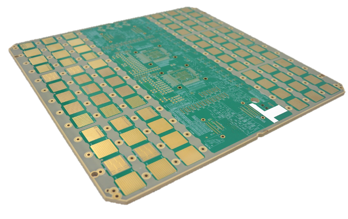
The Backbone of Semiconductor Testing
As semiconductors become more powerful and complex, the equipment needed to test these components must evolve to match. Automated Test Equipment (ATE) PCBs play a central role in this process by connecting chips to testing systems during various stages of production. Understanding these PCBs—and why they matter—can help you ensure your testing processes are as precise and efficient as possible.
What are ATE PCBs?
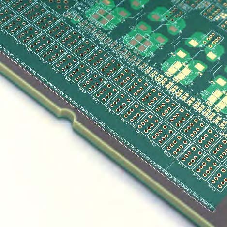
ATE PCBs are complex, high-layer printed circuit boards designed to test semiconductor devices during various stages of manufacturing. Whether testing wafers, packaged ICs (Integrated Circuits), or performing stress tests, ATE PCBs ensure that only high-performing chips reach the market. Their precision, reliability, and durability make them indispensable for semiconductor manufacturers.

ATE Manufacturing Features
Advanced Material Selection
Materials like Megtron 6 and HTG FR4 are chosen for their thermal stability and low signal loss. These materials ensure that the board can handle the high-speed signals required for modern semiconductor testing.
High Layer Count
ATE PCBs often feature 50 or more layers. These layers allow for the complex interconnections needed to test today’s sophisticated chips.
Durable & Conductive Surface Finishes
The board is often finished with Flash Gold or Selective Hard Gold. These finishes ensure that the board can withstand the repeated cycles of testing, where connectors are frequently inserted and removed, while maintaining excellent electrical performance.
Signal Integrity
Ensuring that signals pass through the board without interference or loss is crucial for reliable testing. Advanced PCB materials, tight spacing between traces, and controlled layer-to-layer registration help maintain signal integrity throughout the testing process.
Z-Axis Interconnects (Via Bond)
This technology allows multiple subs to be bonded together, creating a robust Z-axis connection. Via Bond technology simplifies the construction of very high layer count boards (70+ layers) by reducing lamination cycles, shortening lead times, and lowering costs.
Pulse Plating for High Aspect Ratio
Reverse pulse plating enables the plating of very high aspect ratio holes using periodic pulses of opposite polarity, resulting in hole walls with excellent copper uniformity.
ENCAP Technology
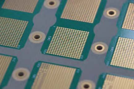
ENCAP (Electrolytic Ni/Au Plating) eliminates the overhang of nickel and gold on contact pads, reducing the risk of shorts or damaged pads during testing. This is especially critical for boards with fine-pitch BGAs (≤0.5mm).
Ultra Flatness Control
Maintaining board flatness is crucial in ATE PCBs, particularly in probe cards and load boards, where even slight warping can cause test inaccuracies. Sunshine achieves ultra-flat planarization with a tolerance of ≤50μm at the DUT (Device Under Test) area, ensuring consistent, reliable test results.
Types of ATE PCBs:
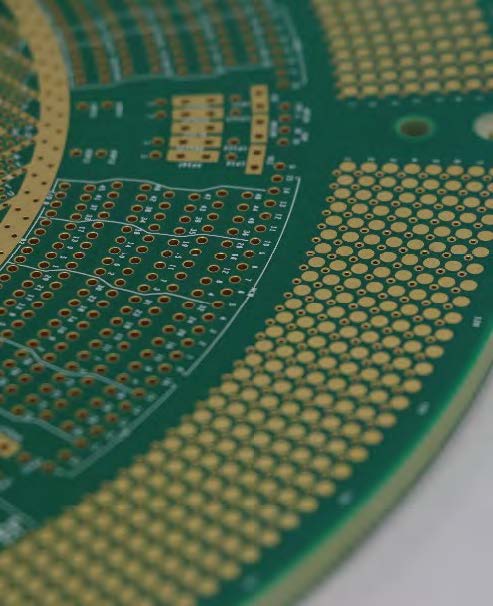
Probe Cards
Precision Testing at the Wafer Level
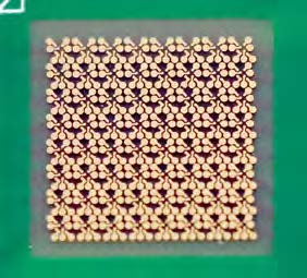
Probe cards test individual dies on a wafer before they are cut and packaged. These cards use a dense array of probes to make electrical contact with the bonding pads of each die. Given the need to test increasingly complex chips, probe cards are often designed with fine-pitch connections and tight impedance control.
Key Features of Probe Cards
- High-Density Connections: Probes must establish numerous precise connections, often with BGA pitches of less than 0.3mm.
- Durability: The probes must be durable enough to withstand repeated contact with the wafer over hundreds or even thousands of test cycles.
- Flatness and Precision: Ensuring that the probe card is perfectly flat is crucial. Even a slight warp or misalignment can lead to inaccurate test results.
- Material: Advanced materials like Megtron 6 provide the necessary thermal and electrical stability to handle high-speed signals during testing.
Check out this helpful little video on Probe Cards.
-2")
Sunshine Global Circuits ATE Probe Card – 2
Sunshine Global Circuits ATE Probe Card – 1
Sunshine Global Circuits ATE Probe Card – 3
Sunshine Global Circuits ATE Probe Card – R1
Sunshine Global Circuits ATE Probe Card – R2
Sunshine Global Circuits ATE Probe Card – 5
Burn-In Boards (BIBs)
Stress Testing for Reliabiability
Burn-In Boards (BIBs) stress test packaged ICs to detect “infant mortality” failures. These boards expose ICs to prolonged high-temperature cycles or repeated power on/off cycling, simulating aging to ensure the chips are reliable before they’re deployed in critical applications like automotive systems.
Key Features of Burn-In Boards
- Thermal Stability: BIBs are designed to withstand high temperatures and repeated heating/cooling cycles. Materials like Polyimide and BT ensure the board withstands repeated high temperatures without degradation.
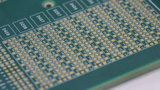
- High Pin Count: BIBs often handle large numbers of devices at once, requiring precise connections to each IC.
- Durability: Given the extended test cycles, BIBs need to be robust enough to perform reliably across many cycles without warping, delaminating, or losing electrical performance.
- Accuracy Under Stress: Maintaining signal integrity while ICs are subjected to thermal stress is key. Tight impedance control helps ensure that the testing environment remains consistent, even as the ICs heat up.

Sunshine Global Circuits ATE Burn In Board 3

Sunshine Global Circuits ATE Burn In Board 2
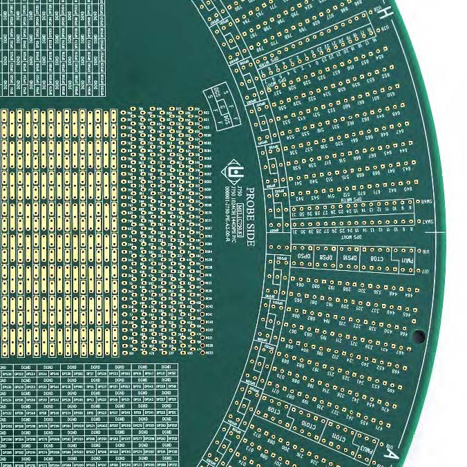
Load Boards
Ensuring Post-Packaging Functionality
Load Boards test packaged ICs for functional performance after assembly. These boards simulate the real-world operating conditions of the chip and verify electrical functionality, speed, and signal integrity. They are often used in final testing before shipment to ensure the device meets specifications.
Key Features of Load Boards
- Impedance Control: Load boards need precise impedance control to handle high-speed or high-frequency signals, ensuring no signal degradation occurs.
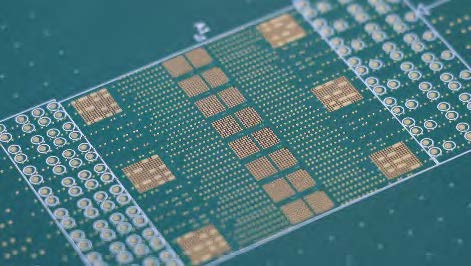
- BGA and Fine-Pitch Compatibility: Many ICs, especially high-performance ones, are packaged using Ball Grid Array (BGA) technology or have fine-pitch connectors. Load boards are designed to accommodate these packaging methods with fine-pitch and BGA test sockets.
- Durability and Reusability: Load boards must be built to handle repeated test cycles without degrading. Materials like Megtron 6 and gold surface finishes ensure that the board can be reused for multiple test runs while maintaining high electrical performance.
- Custom Test Solutions: Load boards are often customized to meet the specific needs of different chips. For example, some may require specialized high-power circuits or multi-chip configurations for testing advanced ICs.
-1_Nvidia")
Sunshine Global Circuits ATE Load Board_TUF 2
Sunshine Global Circuits ATE Load Board 2
Sunshine Global Circuits ATE Load Board 5
Sunshine Global Circuits ATE Load Board 4
Applications for ATE PCBs
ATE PCBs are indispensable in industries that rely on semiconductor chips. From consumer electronics to automotive and telecommunications, these boards ensure that the chips powering everyday devices perform flawlessly.
Semiconductor Fabrication
ATE PCBs test wafers and packaged ICs to ensure they meet design specifications before moving to the next stage of production. Probe cards test each die on a wafer to identify those that are ready for packaging.
Telecommunications
ATE PCBs are used to test high-speed networking ICs and other components that ensure reliable communication in data centers, 5G networks, and other infrastructure.
Consumer Electronics
In devices like smartphones and laptops, every IC goes through rigorous testing on ATE PCBs to ensure it meets speed, power, and efficiency requirements.
Automotive
With the increasing use of semiconductor chips in automotive electronics, from engine controls to infotainment systems, ATE PCBs help ensure that these components perform reliably under demanding conditions.
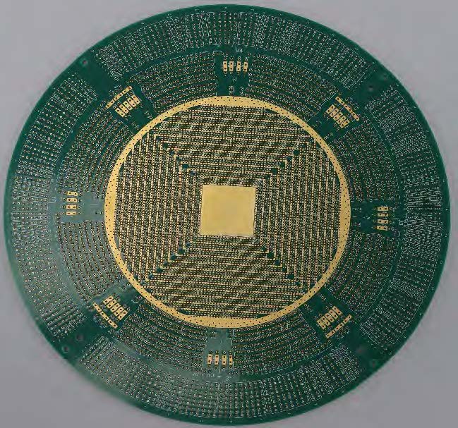
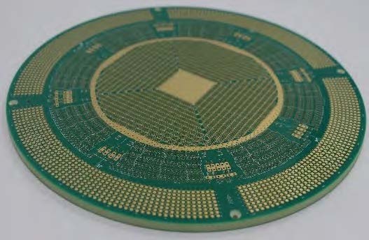
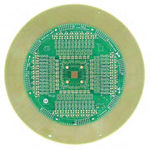
Use Case
Sunshine’s Advanced 64-Layer Vertical Probe Card
Sunshine Global Circuits’ 64-layer board is used as a Vertical Probe Card in semiconductor testing. The probe card is responsible for testing each die on a semiconductor wafer before the dies are cut and packaged. By ensuring that only functional dies are packaged, manufacturers can reduce waste, lower costs, and improve the overall quality of their semiconductor products.
")
Specifications:
- Layer Count: 64 layers of interconnected circuits allow the board to handle the vast number of signals necessary to test semiconductor wafers with high precision.
- Material: The board is made with a combination of Megtron 6 and HTG FR4. These materials offer excellent thermal stability and low signal loss, ensuring the board can handle high-speed signals with minimal distortion.
- Board Thickness: 6.35mm thick to support the 64 layers while maintaining structural integrity.
- Drill Size: 0.2mm drill holes allow for tightly packed circuits, crucial for testing today’s high-density chips.
- Aspect Ratio: 32:1, meaning the thickness of the board is 32 times the drill hole diameter. This high ratio requires advanced drilling technology to ensure reliability.
- BGA Pitch: 0.65mm. This small pitch allows the board to accommodate ball grid arrays, which are commonly used to attach high-performance chips to the board.
- Copper Thickness: 1oz for both inner and outer layers, ensuring robust current-carrying capacity and signal transmission.
- Surface Finishes: The use of Flash Gold and Selective Hard Gold ensures durability and excellent electrical connections during repeated testing cycles.
- Warpage: With a warpage tolerance of just 0.30%, this board maintains a flat surface for accurate and reliable testing.
- DUT Flatness: 50μm flatness ensures the device under test maintains consistent contact with the test probes, which is crucial for precise testing.
Why Choose Sunshine ATE PCBs?
Sunshine Global Circuits offers industry-leading expertise in ATE PCB manufacturing. Our advanced technologies, precise manufacturing processes, and use of high-performance materials ensure our ATE PCBs meet the highest standards for reliability, signal integrity, and durability.
With capabilities including:
- Layer counts up to 60+
- Advanced materials like Megtron 6 and HTG FR4
- Ultra-flat board construction with stringent control over impedance and warpage
- High aspect ratio vias with uniform copper plating
Get a Quote or Sample Today!
At Selmark, we’re providing critical solutions that empower your success. Partner with us to unlock the innovation, reliability, and performance in your designs.
No matter your need, we will help determine the best product for your application or assist in the creation of custom-made designs. Contact us for samples and pricing.
Why Sunshine Global Circuits?
SGC is a PCB manufacturer with a focus on high mix, high technology, and high quality circuit boards. They offer a wide array of products and capabilities, including 2L-36L rigid-PCB’s, HDI & stacked micro-vias, hi-speed and low-loss boards, heavy copper, rigid-flex & flex circuits, metal-backed PCB’s, and RF microwave boards.
We are proud to offer Sunshine products to our customers throughout New England.